Stacked Dies And Methods For Forming Bonded Structures
Patent No. US10879226 (titled "Stacked Dies And Methods For Forming Bonded Structures") was filed by Adeia Semiconductor Bonding Technologies Inc on Feb 7, 2019.
What is this patent about?
’226 is related to the field of three-dimensional (3D) integrated circuit packaging. This involves stacking multiple integrated circuit dies to increase density and performance. A key challenge is managing stress and potential damage to the dies during thinning and stacking processes, especially when using dies from different wafers or with varying thicknesses. Conventional methods often suffer from low product yield due to stress-induced damage during assembly.
The underlying idea behind ’226 is to protect integrated circuit dies during thinning and stacking by applying a protective material around the dies. This material acts as a buffer, preventing damage to the die edges during processes like grinding or polishing. The protective material can comprise one or more layers with specific properties, such as high Young's modulus, matched thermal expansion coefficient, and high glass transition temperature, to withstand subsequent high-temperature processing.
The claims of ’226 focus on methods for packaging integrated device dies that involve directly bonding singulated dies to a carrier, thinning the dies, applying a protective material including to the sidewalls, and then directly bonding a second die to the first. The claims also cover the resulting bonded structure, emphasizing the protective material's role in protecting the die edges and enabling direct bonding without adhesives.
In practice, the invention involves mounting dies to a substrate, thinning them to expose interconnects, and then applying a protective material. This material can be a single layer or multiple layers, such as a thin liner of silicon oxide followed by a filler material. The structure is then planarized, and a second die is directly bonded to the first. This process can be repeated to create multi-layered stacks. The direct bonding process, involving activated surfaces and covalent bonds, ensures strong adhesion between the dies.
’226 differentiates itself from prior approaches by addressing the limitations of conventional die thinning and stacking methods. Unlike adhesive-based stacking, it uses direct bonding to improve electrical and thermal performance. The protective material prevents damage during thinning, allowing for thinner dies and higher stacking densities. Furthermore, the method accommodates dies with different initial thicknesses, increasing flexibility in package design. The use of specific materials with tailored properties ensures the structural integrity of the stacked dies throughout the manufacturing process.
How does this patent fit in bigger picture?
Technical landscape at the time
In the mid-2010s when ’226 was filed, integrated device dies were commonly thinned to enable low-profile packages and three-dimensional integration. At a time when stacking dies with different thicknesses presented alignment challenges, systems commonly relied on techniques to reduce stress during die thinning to prevent damage. Moreover, when material mismatch between dies introduced thermal and chemical bonding challenges, it was non-trivial to efficiently stack integrated device dies with improved yield.
Novelty and Inventive Step
The examiner approved the application because prior art, specifically Nishiyama (US 2002/0004288 A1), failed to disclose or suggest that the dies and carrier are in direct contact. Nishiyama also failed to disclose 'thinning' the plurality of singulated integrated device dies as set forth in the claimed invention which shows, 'after directly bonding dies (3a, 3b) to a carrier (2, 5, 34 in combination) (see Fig. 1A); thinning the dies (3a, 3b) (see Fig. 1B); and providing a protective material (12) on exposed surfaces of the dies including sidewall surfaces of the dies (see Fig. 1C).
Claims
This patent contains 24 claims, of which claims 1, 10, 17, and 23 are independent. The independent claims are directed to methods for packaging integrated device dies and a bonded structure of stacked dies. The dependent claims generally elaborate on the materials, steps, and configurations described in the independent claims.
Key Claim Terms New
Definitions of key terms used in the patent claims.
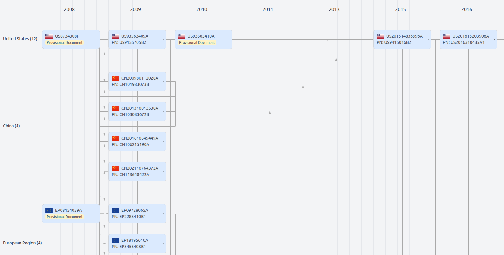
Patent Family

File Wrapper
The dossier documents provide a comprehensive record of the patent's prosecution history - including filings, correspondence, and decisions made by patent offices - and are crucial for understanding the patent's legal journey and any challenges it may have faced during examination.
Date
Description
Get instant alerts for new documents
US10879226
- Application Number
- US16270466
- Filing Date
- Feb 7, 2019
- Status
- Granted
- Expiry Date
- May 19, 2036
- External Links
- Slate, USPTO, Google Patents