Field Programmable Gate Array With External Phase-Locked Loop
Patent No. US10931286 (titled "Field Programmable Gate Array With External Phase-Locked Loop") was filed by Hft Solutions Llc on Jul 23, 2020.
What is this patent about?
’286 is related to the field of field-programmable gate arrays (FPGAs) , specifically addressing the challenge of synchronizing receiver and transmitter clock signals within an FPGA used in high-speed applications like high-frequency trading. Traditional solutions introduce delays due to clock domain crossing circuits, which negatively impacts processing speed. The patent aims to overcome this latency issue.
The underlying idea behind ’286 is to eliminate the need for a clock domain crossing circuit by using an external phase control loop to actively adjust the transmitter clock signal's phase to match the receiver clock signal's phase. This is achieved by feeding back the receiver and transmitter clock signals to an external phase detector and using the detected phase difference to adjust an external adjustable oscillator that drives the transmitter clock generation circuitry.
The claims of ’286 focus on a method for processing a first serial data stream (market data) to generate a second serial data stream (order entry data) using an FPGA system. The method involves receiving the market data and a reference clock signal, deserializing the data, generating a receiver-side clock, performing computations on the data, and then serializing the processed data for transmission. Crucially, the method includes an external phase control loop that adjusts the transmitter-side clock based on a comparison with the receiver-side clock, ensuring phase alignment without a clock domain crossing circuit.
In practice, the FPGA receives high-speed serial data, deserializes it into parallel streams, performs computations (e.g., a trading algorithm), and then serializes the results for transmission. The key is the external phase control circuit, which continuously monitors the phase difference between the receiver and transmitter clocks. This circuit adjusts the frequency or phase of an external oscillator, which in turn affects the transmitter clock signal. This feedback loop ensures that the transmitter clock remains synchronized with the receiver clock, allowing for direct data transfer between clock domains without the added latency of a clock domain crossing circuit.
This approach differentiates itself from prior solutions by moving the phase synchronization mechanism outside the FPGA and implementing it as a closed-loop feedback system. Instead of relying on internal clock domain crossing circuits that inherently introduce delays, ’286 uses an external phase detector, phase controller, and adjustable oscillator to actively align the transmitter and receiver clock phases. This allows for faster processing and reduced latency, which is critical in applications like high-frequency trading where even microsecond delays can have significant consequences.
How does this patent fit in bigger picture?
Technical landscape at the time
In the late 2010s when ’286 was filed, FPGAs were increasingly used in high-speed applications where minimizing latency was critical, at a time when clock domain crossing was a common technique for synchronizing signals between different clock domains within an FPGA, even though such techniques introduced delays. When designing high-throughput systems, engineers commonly relied on phase-locked loops (PLLs) to generate stable clock signals, but synchronizing the phase of clocks between different parts of a system, especially between receiver and transmitter sides, was non-trivial.
Novelty and Inventive Step
The examiner approved the patent because the prior art does not teach or suggest a method for processing a first serial data stream comprising market data, using a field programmable gate array system, to generate a second serial data stream comprising order entry data, wherein the method comprises specific steps related to transmitting a receiver side clock signal to a phase detector external to the FPGA and generating a feedback clock signal using an adjustable oscillator until a phase detector output is below a threshold.
Claims
This patent contains 22 claims, with claim 1 being the only independent claim. Independent claim 1 is directed to a method for processing a first serial data stream comprising market data, using a field programmable gate array system, to generate a second serial data stream comprising order entry data. The dependent claims generally elaborate on and refine the specifics of the method described in the independent claim.
Key Claim Terms New
Definitions of key terms used in the patent claims.
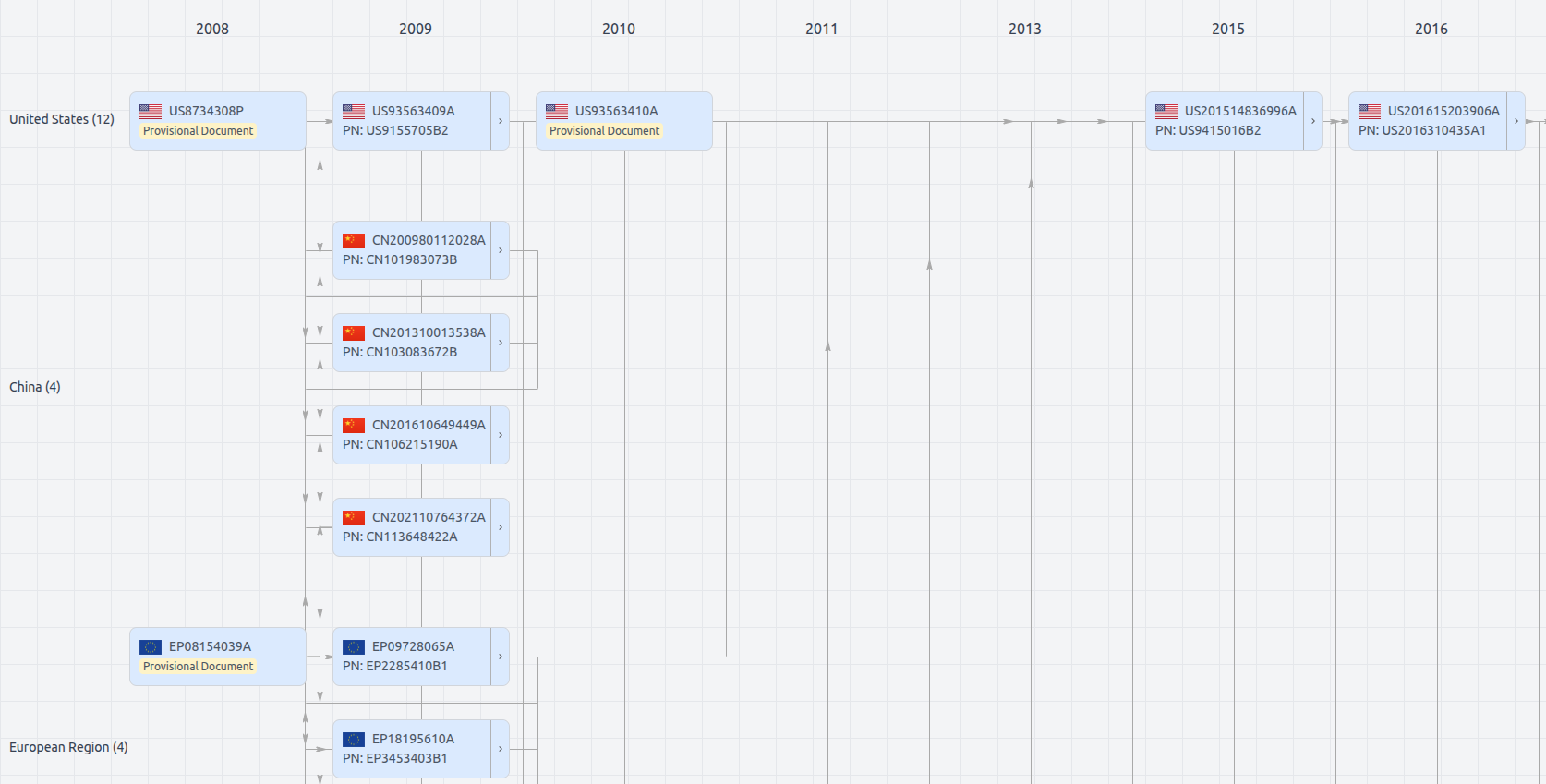
Patent Family

File Wrapper
The dossier documents provide a comprehensive record of the patent's prosecution history - including filings, correspondence, and decisions made by patent offices - and are crucial for understanding the patent's legal journey and any challenges it may have faced during examination.
Get instant alerts for new documents
US10931286
- Application Number
- US16937314
- Filing Date
- Jul 23, 2020
- Status
- Granted
- Expiry Date
- Nov 1, 2039
- External Links
- Slate, USPTO, Google Patents