Dynamic Random Access Memory Applied To An Embedded Display Port

Patent No. US10998017 (titled "Dynamic Random Access Memory Applied To An Embedded Display Port") was filed by Wecrevention Inc on Oct 4, 2018.

What is this patent about?

’017 is related to the field of dynamic random access memory (DRAM), specifically addressing power consumption issues when DRAM is used as a frame buffer in embedded display port (eDP) applications. The background highlights the increasing demand for lower power consumption in timing controllers that utilize frame buffers for panel self-refresh (PSR) functionality in eDP, especially in portable devices.

The underlying idea behind ’017 is to reduce the power consumption of a DRAM used in an eDP by operating its core and peripheral circuits at lower voltages than those specified by JEDEC standards. This is achieved by splitting the DRAM architecture into a memory core and a peripheral circuit , each operating at a voltage below 1.1V. This allows for reduced power consumption in both memory operations and access functions.

The claims of ’017 focus on a DRAM comprising a DRAM core cell and a peripheral circuit. The core cell operates at a first voltage below 1.1V, and the peripheral circuit, connected to the core cell, operates at a second voltage also below 1.1V. The claim specifies that both components are integrated on a single chip, with the peripheral circuit external to the core cell, and that these voltages enable the DRAM's use in an embedded display port.

In practice, this architecture allows for a more efficient power distribution within the DRAM. By reducing the operating voltages of both the memory core and the peripheral circuits, the overall power consumption is significantly lowered. This is particularly beneficial in eDP applications where the DRAM functions as a frame buffer, constantly refreshing the display and thus consuming a considerable amount of power.

This approach differentiates itself from prior solutions by moving away from the standard JEDEC voltage specifications for DRAM operation. Instead of using voltages like 1.8V or higher, ’017 employs sub-1.1V operation for both the core and peripheral circuits. This voltage reduction directly translates to lower power consumption, addressing the specific needs of low-power eDP implementations and extending battery life in portable devices.

How does this patent fit in bigger picture?

Technical landscape at the time

In the early 2010s when ’017 was filed, dynamic random access memory (DRAM) was commonly used as a frame buffer in timing controllers for liquid crystal displays, at a time when panel self-refresh (PSR) functionality was being introduced to reduce GPU power consumption. At that time, memory manufacturers were facing the challenge of reducing the power consumption of the frame buffer itself, as the continuous operation of the DRAM could offset the power savings achieved by the GPU's reduced activity.

Novelty and Inventive Step

The examiner approved the claims because they include a DRAM core cell and a peripheral circuit formed on a single chip, with the peripheral circuit external to the DRAM core cell. The DRAM memory cells operate at a first voltage, and the peripheral circuit operates at a second voltage. These first and second voltages enable the DRAM to be used in an embedded display port (eDP). The examiner stated that prior art references, taken individually or in combination, do not teach or make obvious these limitations.

Claims

This patent has two claims, with claim 1 being independent. Independent claim 1 focuses on a DRAM comprising a DRAM core cell and a peripheral circuit, both operating at voltages below 1.1V, suitable for an embedded display port. Dependent claim 2 builds upon claim 1 by adding an input/output unit operating at a voltage below 1.1V.

Key Claim Terms New

Definitions of key terms used in the patent claims.

Term (Source)Support for SpecificationInterpretation
Dram core cell
(Claim 1)
“As shown in Table II, operation voltages of the memory core unit 102 in the DDR I specification, the low power DDR I specification, the DDR II specification, and the low power DDR II specification are a first predetermined voltage, where the first predetermined voltage is lower than 1.1V; operation voltages of the peripheral circuit unit 104 in the DDR I specification, the low power DDR I specification, the DDR II specification, and the low power DDR II specification are a second predetermined voltage, where the second predetermined voltage is lower than 1.1V; and operation voltages of the input/output unit 106 in the DDR I specification, the low power DDR I specification, the DDR II specification, and the low power DDR II specification are a third predetermined voltage, where the third predetermined voltage is lower than 1.1V.”A volatile memory cell within the dynamic random access memory that operates at a first voltage.
Embedded display port
(Claim 1)
“An embedded display port (eDP) published by the Video Electronics Standards Association (VESA) is used for acting as a standard display panel interface to connect external devices. For example, the embedded display port can act as an interface between a video card and a notebook panel. In addition, the embedded display port version 1.3 published by the Video Electronics Standards Association adds a panel self refresh (PSR) function, where the panel self refresh function can make a graphic processing unit (GPU) turn off connection between the graphic processing unit and a liquid crystal panel when a frame displayed on the liquid crystal panel is frozen.”An interface to connect external devices, such as between a video card and a notebook panel.
First voltage range
(Claim 1)
“As shown in Table II, operation voltages of the memory core unit 102 in the DDR I specification, the low power DDR I specification, the DDR II specification, and the low power DDR II specification are a first predetermined voltage, where the first predetermined voltage is lower than 1.1V; operation voltages of the peripheral circuit unit 104 in the DDR I specification, the low power DDR I specification, the DDR II specification, and the low power DDR II specification are a second predetermined voltage, where the second predetermined voltage is lower than 1.1V; and operation voltages of the input/output unit 106 in the DDR I specification, the low power DDR I specification, the DDR II specification, and the low power DDR II specification are a third predetermined voltage, where the third predetermined voltage is lower than 1.1V.”A voltage range within which the DRAM core cell operates, where the first voltage is lower than 1.1V.
Peripheral circuit
(Claim 1)
“As shown in the FIGURE, the dynamic random access memory 100 includes a memory core unit 102, a peripheral circuit unit 104, and an input/output unit 106, where the peripheral circuit unit 104 is electrically connected to the memory core unit 102, and the input/output unit 106 is electrically connected to the peripheral circuit unit 104 and the memory core unit 102. As shown in Table II, operation voltages of the memory core unit 102 in the DDR I specification, the low power DDR I specification, the DDR II specification, and the low power DDR II specification are a first predetermined voltage, where the first predetermined voltage is lower than 1.1V; operation voltages of the peripheral circuit unit 104 in the DDR I specification, the low power DDR I specification, the DDR II specification, and the low power DDR II specification are a second predetermined voltage, where the second predetermined voltage is lower than 1.1V; and operation voltages of the input/output unit 106 in the DDR I specification, the low power DDR I specification, the DDR II specification, and the low power DDR II specification are a third predetermined voltage, where the third predetermined voltage is lower than 1.1V.”A circuit electrically connected to the DRAM core cell that operates at a second voltage, and is external to the DRAM core cell.
Second voltage range
(Claim 1)
“As shown in Table II, operation voltages of the memory core unit 102 in the DDR I specification, the low power DDR I specification, the DDR II specification, and the low power DDR II specification are a first predetermined voltage, where the first predetermined voltage is lower than 1.1V; operation voltages of the peripheral circuit unit 104 in the DDR I specification, the low power DDR I specification, the DDR II specification, and the low power DDR II specification are a second predetermined voltage, where the second predetermined voltage is lower than 1.1V; and operation voltages of the input/output unit 106 in the DDR I specification, the low power DDR I specification, the DDR II specification, and the low power DDR II specification are a third predetermined voltage, where the third predetermined voltage is lower than 1.1V.”A voltage range within which the peripheral circuit operates, where the second voltage is lower than 1.1V.

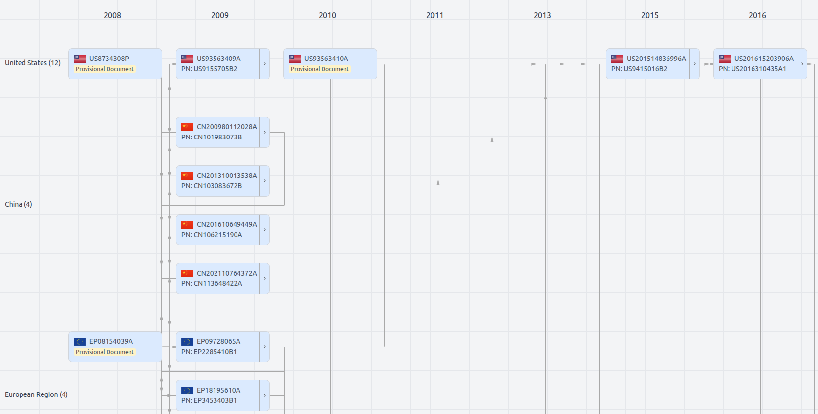
Patent Family

Patent Family

File Wrapper

The dossier documents provide a comprehensive record of the patent's prosecution history - including filings, correspondence, and decisions made by patent offices - and are crucial for understanding the patent's legal journey and any challenges it may have faced during examination.

  • Date

    Description

  • Get instant alerts for new documents

US10998017

WECREVENTION INC
Application Number
US16151347
Filing Date
Oct 4, 2018
Status
Granted
Expiry Date
Jun 19, 2033
External Links
Slate, USPTO, Google Patents