Field Programmable Gate Array With External Phase-Locked Loop

Patent No. US11128305 (titled "Field Programmable Gate Array With External Phase-Locked Loop") was filed by Hft Solutions Llc on Jan 19, 2021.

What is this patent about?

’305 is related to the field of field-programmable gate arrays (FPGAs) , specifically addressing the challenge of synchronizing receiver and transmitter clock signals within the FPGA. Traditional approaches introduce delays due to clock domain crossing circuits, which is undesirable in high-speed applications like high-frequency trading where microsecond-level accuracy is crucial.

The underlying idea behind ’305 is to eliminate the need for a clock domain crossing circuit by using an external phase control circuit to actively adjust the transmitter clock signal's phase. This is achieved by comparing the receiver and transmitter clock phases, generating adjustment information, and using an adjustable oscillator to modify the transmitter clock signal until it is phase-aligned with the receiver clock.

The claims of ’305 focus on a field programmable gate array system comprising an FPGA and an external phase control circuit. The FPGA includes a deserializer to convert a serial data stream into parallel data streams and generate a receiver-side clock, computational circuitry to process the parallel data, and a serializer to convert the processed parallel data back into a serial data stream and generate a transmitter-side clock. The external phase control circuit compares the receiver and transmitter clock phases and adjusts the transmitter clock signal.

In practice, the FPGA receives a serial data stream and a reference clock signal. The deserializer converts the serial data into parallel streams and generates a receiver-side clock. The computational circuitry processes the data without clock domain crossing. The serializer converts the processed data back to serial form, generating a transmitter-side clock. The external phase control circuit, including a phase detector, phase controller, and adjustable oscillator, continuously monitors and adjusts the transmitter clock's phase to match the receiver clock's phase, ensuring phase alignment .

This approach differs from prior solutions by moving the phase synchronization mechanism outside the FPGA , thereby avoiding the inherent latency associated with on-chip clock domain crossing circuits. By using an external adjustable oscillator and a feedback loop, the system dynamically adjusts the transmitter clock signal to maintain phase alignment with the receiver clock signal, enabling faster processing and reduced latency, which is critical for applications requiring high-speed data processing and minimal delay.

How does this patent fit in bigger picture?

Technical landscape at the time

In the late 2010s when ’305 was filed, FPGAs were increasingly used in high-performance computing applications at a time when clock domain crossing was a common technique for synchronizing signals between different clock domains within the FPGA. However, when systems commonly relied on clock domain crossing, this introduced latency, which was undesirable for applications requiring precise timing.

Novelty and Inventive Step

The examiner approved the patent because the prior art did not teach or suggest a field programmable gate array system that includes computational circuitry connected to a deserializer for receiving parallel data streams and a receiver-side clock signal, along with a serializer connected to the computational circuitry. The serializer receives parallel data streams from the computational circuitry and transmits a transmitter-side clock signal back to the computational circuitry. The prior art also failed to teach a phase control circuit located outside the FPGA, which includes a phase detector that compares the receiver-side clock signal to a third signal and generates a phase difference indicator signal based on the comparison.

Claims

There are 22 claims in total, with claim 1 being the only independent claim. Independent claim 1 is directed to a field programmable gate array system with a phase control circuit. The dependent claims generally elaborate on and add detail to the elements and features described in the independent claim.

Key Claim Terms New

Definitions of key terms used in the patent claims.

Term (Source)Support for SpecificationInterpretation
Adjustable oscillator
(Claim 1)
“In embodiments, a field programmable gate array system includes (b) a phase control circuit, provided outside of the field programmable gate array, wherein the phase control circuit includes: (3) an adjustable oscillator operationally connected to the phase controller and configured to receive the adjustment information as well as operationally connected to the second reference clock pin of the first interface of the field programmable gate array, wherein the adjustable oscillator is configured to generate the second clock signal including the second frequency and the second phase based on the adjustment information and transmit the second clock signal to the second reference clock pin of the first interface of the field programmable gate array”A component of the phase control circuit that receives adjustment information from the phase controller and generates the second clock signal based on this information. The second clock signal is then transmitted to the second reference clock pin of the FPGA.
First receiver side clock signal
(Claim 1)
“In embodiments, a field programmable gate array system includes (a) a field programmable gate array comprising (2) a deserializer operationally connected to: (x) the first reference clock pin to receive as a first input the first clock signal and (y) the first plurality of data pins to receive as a second input the first serial data stream, and wherein the deserializer is configured to: (B) generate a first receiver side clock signal based on the first clock signal, wherein the first receiver side clock signal has a third frequency and a third phase; and (C) transmit the first plurality of parallel data streams and the first receiver side clock signal within the field programmable gate array; (5) a second interface including: (A) a first clock output pin configured to transmit the first receiver side clock signal, wherein the first clock output pin is operationally connected to the deserializer.”A clock signal generated by the deserializer based on the first clock signal, having a third frequency and a third phase. This signal is transmitted within the field programmable gate array and outputted via the first clock output pin.
First set of operations
(Claim 1)
“In embodiments, a field programmable gate array system includes (a) a field programmable gate array comprising (3) computational circuitry operationally connected to the deserializer to receive the first plurality of parallel data streams and the first receiver side clock signal, wherein the computational circuitry is configured to perform a first set of operations on the first plurality of parallel data streams to generate a second plurality of parallel processed data streams having a second amount of data streams and the computational circuitry performs the first set of operations to generate the second plurality of parallel processed data without use of a clock domain crossing circuit”Operations performed by the computational circuitry on the first plurality of parallel data streams to generate a second plurality of parallel processed data streams. These operations are performed without the use of a clock domain crossing circuit.
First wire rate clock signal
(Claim 1)
“In embodiments, a field programmable gate array system includes (a) a field programmable gate array comprising (4) a serializer operationally connected to: (x) the second reference clock pin to receive as a third input a first wire rate clock signal based on the second clock signal, wherein the first wire rate clock signal has a fourth frequency and a fourth phase; (y) the second plurality of data pins to transmit as a first output the second serial data stream; (z) the computational circuitry, wherein the serializer receives the second plurality of parallel processed data streams from the computational circuitry and the serializer transmits to the computational circuitry a first transmitter side clock signal including a fifth frequency and a fifth phase”A clock signal, based on the second clock signal, having a fourth frequency and a fourth phase, received by the serializer. The serializer generates the first transmitter side clock signal based on this signal.
Phase difference indicator signal
(Claim 1)
“In embodiments, a field programmable gate array system includes (b) a phase control circuit, provided outside of the field programmable gate array, wherein the phase control circuit includes: (1) a phase detector operationally connected to the first clock output pin and the second clock output pin of the second interface of the field programmable gate array, and wherein the phase detector is configured to compare the third phase of the receiver side clock signal to the fifth phase of the transmitter side clock signal and to generate a phase difference indicator signal based on a difference between the third phase of the receiver side clock signal and the fifth phase of the transmitter side clock signal; (2) a phase controller operationally connected to the phase detector and configured to receive the phase difference indicator signal, and wherein the phase controller is configured to determine adjustment information based on the phase difference indicator signal”A signal generated by the phase detector based on a difference between the third phase of the receiver side clock signal and the sixth phase of the third clock signal. This signal is received by the phase controller.

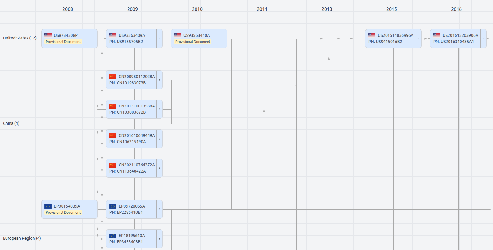
Patent Family

Patent Family

File Wrapper

The dossier documents provide a comprehensive record of the patent's prosecution history - including filings, correspondence, and decisions made by patent offices - and are crucial for understanding the patent's legal journey and any challenges it may have faced during examination.

  • Date

    Description

  • Get instant alerts for new documents

US11128305

HFT SOLUTIONS LLC
Application Number
US17248304
Filing Date
Jan 19, 2021
Status
Granted
Expiry Date
Nov 1, 2039
External Links
Slate, USPTO, Google Patents