Flash-Dram Hybrid Memory Module
Patent No. US11232054 (titled "Flash-Dram Hybrid Memory Module") was filed by Netlist Inc on May 24, 2021.
What is this patent about?
’054 is related to the field of computer memory, specifically memory modules that combine different types of memory, such as Flash and DRAM, to improve performance. Traditional memory systems often face bottlenecks due to the speed disparity between the CPU and storage devices. Hybrid memory modules aim to bridge this gap by leveraging the speed of DRAM for buffering and the non-volatility of Flash for persistent storage, but prior solutions have suffered from limitations in write speeds and CPU bus utilization.
The underlying idea behind ’054 is to create a hybrid memory module with both DRAM and Flash memory, managed by an on-module controller and a data manager. This architecture allows for intelligent data transfer between the host system, DRAM, and Flash, optimizing for both read and write operations. The key insight is to use the DRAM as a high-speed buffer for the Flash, enabling the host system to interact primarily with the DRAM, thereby mitigating the slower access times of the Flash memory.
The claims of ’054 focus on a memory module comprising a printed circuit board with an interface for connecting to a host system. The module includes a voltage conversion circuit with at least three buck converters to generate regulated voltages. These voltages power various components, including SDRAM devices. A controller with a voltage monitor detects changes in the input voltage and initiates actions like transferring data to non-volatile memory.
In practice, the memory module operates by receiving commands from the host system, which are interpreted by the on-module controller. The controller then directs the data manager to move data between the Flash and DRAM based on the command type and data location. For read operations, data is pre-fetched from Flash to DRAM, allowing the host to read from the faster DRAM. For write operations, data is initially written to DRAM and later transferred to Flash, with the controller managing the data flow and ensuring data integrity.
This approach differs from prior solutions by providing a more transparent and efficient interface between the host system and the hybrid memory. Unlike systems where the host directly manages both DRAM and Flash address spaces, ’054 presents a unified memory space, simplifying memory management for the host. Furthermore, the use of a dedicated data manager allows for on-the-fly data formatting and error correction, improving overall system reliability and performance by hiding the Flash memory from the host.
How does this patent fit in bigger picture?
Technical landscape at the time
In the mid-2000s when ’054 was filed, memory systems commonly relied on separate DRAM and Flash memory components, at a time when hybrid memory solutions faced hardware and software constraints that made efficient data transfer between different memory types non-trivial. Systems typically relied on CPU I/O channels for data transfers, which created a bottleneck between the high-speed CPU and slower storage or memory subsystems.
Novelty and Inventive Step
The examiner approved the application because the prior art of record did not teach or suggest a voltage conversion circuit coupled to the PCB and configured to provide at least three regulated voltages, wherein the voltage conversion circuit includes at least three buck converters each of which is configured to produce a regulated voltage of the at least three regulated voltages. Also, the prior art did not teach or suggest a controller coupled to the PCB, the controller including a voltage monitor circuit coupled to an input voltage received from the host system via the interface, the voltage monitor circuit configured to detect an amplitude change in the input voltage, wherein, in response to the voltage monitor detecting an amplitude change in the input voltage, the memory module transitions from a first operable state to a second operable state.
Claims
This patent includes 30 claims, with independent claims numbered 1, 16, and 24. The independent claims generally focus on a memory module comprising a printed circuit board, a voltage conversion circuit with buck converters, SDRAM devices, and a controller with a voltage monitor. The dependent claims generally elaborate on the specifics of the voltage amplitudes, voltage monitoring, operable states, pre-regulated voltages, and diode configurations within the memory module.
Key Claim Terms New
Definitions of key terms used in the patent claims.
Litigation Cases New
US Latest litigation cases involving this patent.
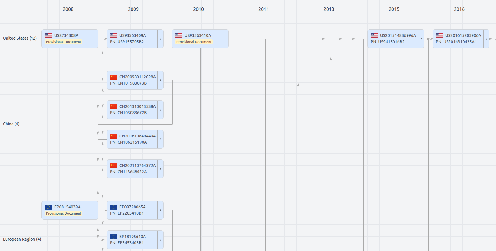
Patent Family

File Wrapper
The dossier documents provide a comprehensive record of the patent's prosecution history - including filings, correspondence, and decisions made by patent offices - and are crucial for understanding the patent's legal journey and any challenges it may have faced during examination.
Date
Description
Get instant alerts for new documents
US11232054
- Application Number
- US17328019
- Filing Date
- May 24, 2021
- Status
- Granted
- Expiry Date
- Jun 2, 2028
- External Links
- Slate, USPTO, Google Patents