Methods For Producing A 3D Semiconductor Memory Device And Structure
Patent No. US11342214 (titled "Methods For Producing A 3D Semiconductor Memory Device And Structure") was filed by Monolithic 3D Inc on Mar 10, 2022.
What is this patent about?
’214 is related to the field of 3D integrated circuits , specifically focusing on the fabrication of 3D memory devices. The background involves the increasing demand for higher memory density and performance, which traditional 2D scaling struggles to meet. 3D integration offers a solution by stacking multiple layers of memory cells vertically, but this presents challenges in manufacturing and thermal management.
The underlying idea behind ’214 is to create a 3D memory device by sequentially building multiple levels of memory cells above a base layer containing transistors and metal interconnects. This is achieved through controlled etching and deposition processes, allowing for the creation of vertically stacked memory cells with individual memory transistors in each level. The process aims to maximize memory density while maintaining manufacturability.
The claims of ’214 focus on a method for producing a 3D memory device. The method involves providing a base level with a single crystal layer and transistors, then forming subsequent levels above it. Each level is etched to create holes, and memory cells are formed within these levels, each cell having its own memory transistor. The claims also cover adjusting the annealing of the base transistors to account for the thermal budget of the memory transistor processing, and forming tungsten vias through the stacked levels.
In practice, the invention involves a layer-by-layer fabrication process. A base layer containing transistors and metal interconnects is created. Then, additional layers are formed on top, with each layer etched to create openings for memory cells. Memory transistors are then formed within these openings. The process is repeated to create multiple levels of memory cells, increasing the overall memory density. The use of single crystal silicon for the transistor channels ensures high performance.
’214 differentiates itself from prior approaches by focusing on a sequential, layer-by-layer fabrication process that allows for precise control over the formation of memory cells in each level. This approach enables the creation of high-density 3D memory devices while addressing thermal management concerns through thermal budget considerations during transistor annealing. The use of tungsten vias provides reliable electrical connections between the stacked layers.
How does this patent fit in bigger picture?
Technical landscape at the time
In the late 2010s when ’214 was filed, 3D IC design and fabrication was an active area of research, at a time when stacking multiple layers of transistors and memory cells was typically implemented using techniques that required careful management of thermal budgets and material compatibility. When forming contacts to transistors, systems commonly relied on silicides to reduce contact resistance, but hardware or software constraints made it non-trivial to optimize silicide work functions for different transistor types in 3D structures.
Novelty and Inventive Step
The examiner approved the application because the prior art neither anticipates nor renders obvious the claimed subject matter. Specifically, the prior art does not teach forming a first and second metal layer where the first level includes transistors and the metal layers, and then forming at least one second level above the second metal layer.
Claims
This patent contains 21 claims, with independent claims numbered 1, 8, and 15. The independent claims are generally directed to methods for producing 3D memory devices. The dependent claims generally elaborate on and add detail to the methods described in the independent claims.
Key Claim Terms New
Definitions of key terms used in the patent claims.
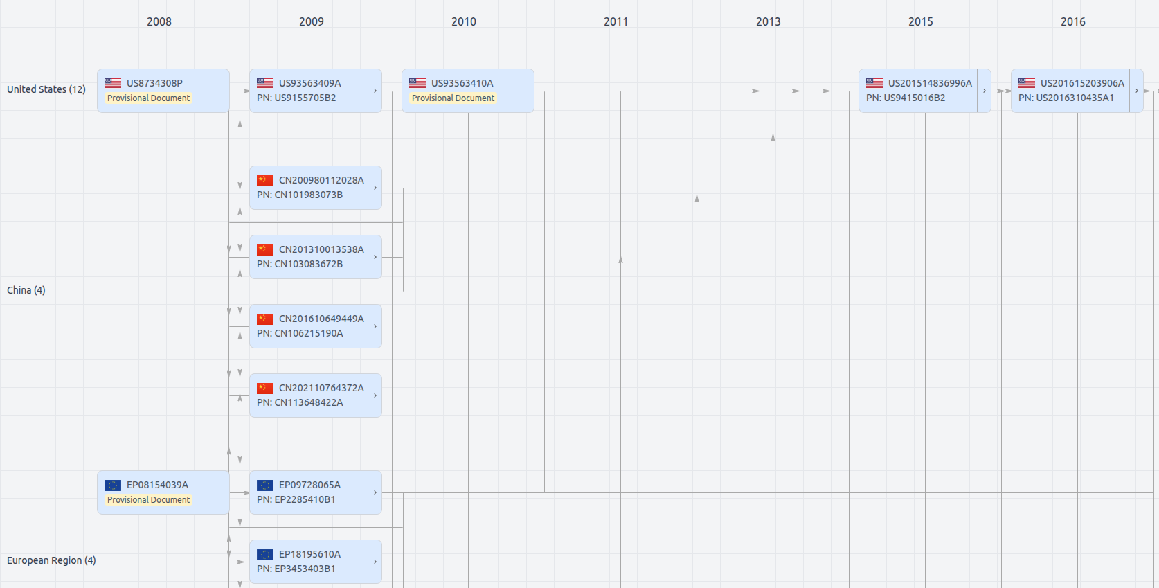
Patent Family

File Wrapper
The dossier documents provide a comprehensive record of the patent's prosecution history - including filings, correspondence, and decisions made by patent offices - and are crucial for understanding the patent's legal journey and any challenges it may have faced during examination.
Date
Description
Get instant alerts for new documents
US11342214
- Application Number
- US17692146
- Filing Date
- Mar 10, 2022
- Status
- Granted
- Expiry Date
- Nov 18, 2030
- External Links
- Slate, USPTO, Google Patents