Method For Producing A 3D Semiconductor Device And Structure With Single Crystal Transistors And Metal Gate Electrodes

Patent No. US11610802 (titled "Method For Producing A 3D Semiconductor Device And Structure With Single Crystal Transistors And Metal Gate Electrodes") was filed by Monolithic 3D Inc on Jun 22, 2022.

What is this patent about?

’802 is related to the field of 3D integrated circuits and, more specifically, to methods for fabricating such circuits with multiple levels of memory cells. The background acknowledges the increasing demand for multilayer or 3D ICs, particularly for custom products, and the challenges associated with their fabrication, such as high mask-set costs and limited flexibility. The patent aims to address these challenges by providing methods for creating 3D semiconductor devices with improved structuring and fabrication techniques.

The underlying idea behind ’802 is to create a 3D memory device by stacking multiple layers of memory cells on top of a base layer containing peripheral circuitry. The key insight is to deposit the gate electrodes for transistors in different memory layers simultaneously. This simplifies the fabrication process and potentially improves alignment between the layers.

The claims of ’802 focus on a method for producing a 3D semiconductor device. This involves providing a base level with a single crystal layer, forming peripheral circuits with transistors on this base, adding metal layers for interconnect, and then creating at least two additional levels for memory cells. A key aspect is the simultaneous deposition of gate electrodes for transistors in the different memory levels, achieved after performing separate lithography steps on each memory level.

The implementation involves a sequential build-up of layers, starting with a single-crystal base for peripheral circuitry. Metal layers provide interconnect. Memory cell layers are then added, each undergoing lithography. The crucial step is the simultaneous gate electrode deposition, which streamlines the process. This contrasts with prior approaches that might involve separate gate depositions for each layer, potentially increasing complexity and cost.

This approach allows for a more efficient fabrication process by reducing the number of deposition steps. By depositing the gate electrodes simultaneously, the patent aims to improve alignment and reduce manufacturing costs. The use of a single crystal base layer ensures high-performance transistors for the peripheral circuitry, while the stacked memory layers increase the overall memory density of the device. The simultaneous gate deposition is a key differentiator from prior art.

How does this patent fit in bigger picture?

Technical landscape at the time

In the late 2010s when '802 was filed, at a time when 3D integrated circuits were gaining traction, forming multi-layer memory structures was an area of active development. It was common to form transistors on multiple levels and interconnect them using metal layers. Lithography steps were essential for defining the patterns on each layer. Deposition and etching processes were also crucial for forming the various layers and structures of the 3D IC.

Novelty and Inventive Step

The examiner approved the application because the prior art, whether considered individually or in combination, did not disclose or suggest all the claimed elements and limitations. Specifically, the examiner noted the absence of teachings related to performing a first lithography step on a second level, forming a third level above the second, performing a second lithography step on the third level, forming first memory cells within the second level and second memory cells within the third level using deposition and etch processes, where each memory cell includes at least one transistor, and then simultaneously depositing gate electrodes on both the second and third transistors.

Claims

This patent contains 20 claims, of which claims 1, 8, and 15 are independent. The independent claims are directed to methods for producing a 3D semiconductor device involving multiple levels, metal layers, lithography steps, and the formation of memory cells with transistors. The dependent claims generally add further detail or limitations to the method steps described in the independent claims.

Key Claim Terms New

Definitions of key terms used in the patent claims.

Term (Source)Support for SpecificationInterpretation
First metal layer
(Claim 1, Claim 8, Claim 15)
“In one aspect, a method for producing a 3D semiconductor device, the method including: providing a first level, the first level including a first single crystal layer; forming peripheral circuitry in and/or on the first level, where the peripheral circuitry includes first single crystal transistors; forming a first metal layer on top of the first level; forming a second metal layer on top of the first metal layer; forming at least one second level disposed on top of or above the second metal layer; performing a first lithography step; forming at least one third level disposed on top of or above the at least one second level; performing a second lithography step; performing additional processing steps to form a plurality of first memory cells within the at least one second level and a plurality of second memory cells within the at least one third level, where each of the plurality of first memory cells includes at least one second transistor, and where each of the plurality of second memory cells includes at least one third transistor; and performing at least one deposition step to deposit a gate electrode for the second transistors and the third transistors.”A metal layer formed on top of the first level.
First single crystal layer
(Claim 1, Claim 8, Claim 15)
“In one aspect, a method for producing a 3D semiconductor device, the method including: providing a first level, the first level including a first single crystal layer; forming peripheral circuitry in and/or on the first level, where the peripheral circuitry includes first single crystal transistors; forming a first metal layer on top of the first level; forming a second metal layer on top of the first metal layer; forming at least one second level disposed on top of or above the second metal layer; performing a first lithography step; forming at least one third level disposed on top of or above the at least one second level; performing a second lithography step; performing additional processing steps to form a plurality of first memory cells within the at least one second level and a plurality of second memory cells within the at least one third level, where each of the plurality of first memory cells includes at least one second transistor, and where each of the plurality of second memory cells includes at least one third transistor; and performing at least one deposition step to deposit a gate electrode for the second transistors and the third transistors.”The base layer of the 3D semiconductor device, made of a single crystal material.
First single crystal transistors
(Claim 1, Claim 8, Claim 15)
“In one aspect, a method for producing a 3D semiconductor device, the method including: providing a first level, the first level including a first single crystal layer; forming peripheral circuitry in and/or on the first level, where the peripheral circuitry includes first single crystal transistors; forming a first metal layer on top of the first level; forming a second metal layer on top of the first metal layer; forming at least one second level disposed on top of or above the second metal layer; performing a first lithography step; forming at least one third level disposed on top of or above the at least one second level; performing a second lithography step; performing additional processing steps to form a plurality of first memory cells within the at least one second level and a plurality of second memory cells within the at least one third level, where each of the plurality of first memory cells includes at least one second transistor, and where each of the plurality of second memory cells includes at least one third transistor; and performing at least one deposition step to deposit a gate electrode for the second transistors and the third transistors.”Transistors made of single crystal material that are part of the peripheral circuitry.
Peripheral circuitry
(Claim 1, Claim 8, Claim 15)
“In one aspect, a method for producing a 3D semiconductor device, the method including: providing a first level, the first level including a first single crystal layer; forming peripheral circuitry in and/or on the first level, where the peripheral circuitry includes first single crystal transistors; forming a first metal layer on top of the first level; forming a second metal layer on top of the first metal layer; forming at least one second level disposed on top of or above the second metal layer; performing a first lithography step; forming at least one third level disposed on top of or above the at least one second level; performing a second lithography step; performing additional processing steps to form a plurality of first memory cells within the at least one second level and a plurality of second memory cells within the at least one third level, where each of the plurality of first memory cells includes at least one second transistor, and where each of the plurality of second memory cells includes at least one third transistor; and performing at least one deposition step to deposit a gate electrode for the second transistors and the third transistors.”Circuitry formed on the first level, comprising single crystal transistors.
Second metal layer
(Claim 1, Claim 8, Claim 15)
“In one aspect, a method for producing a 3D semiconductor device, the method including: providing a first level, the first level including a first single crystal layer; forming peripheral circuitry in and/or on the first level, where the peripheral circuitry includes first single crystal transistors; forming a first metal layer on top of the first level; forming a second metal layer on top of the first metal layer; forming at least one second level disposed on top of or above the second metal layer; performing a first lithography step; forming at least one third level disposed on top of or above the at least one second level; performing a second lithography step; performing additional processing steps to form a plurality of first memory cells within the at least one second level and a plurality of second memory cells within the at least one third level, where each of the plurality of first memory cells includes at least one second transistor, and where each of the plurality of second memory cells includes at least one third transistor; and performing at least one deposition step to deposit a gate electrode for the second transistors and the third transistors.”A metal layer formed on top of the first metal layer.

Patent Family

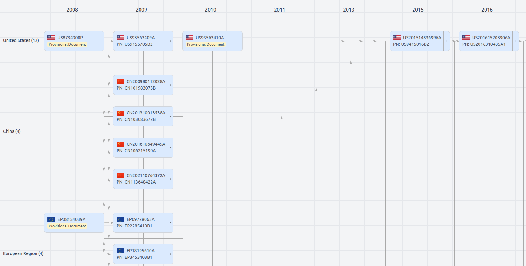
Patent Family

File Wrapper

The dossier documents provide a comprehensive record of the patent's prosecution history - including filings, correspondence, and decisions made by patent offices - and are crucial for understanding the patent's legal journey and any challenges it may have faced during examination.

  • Date

    Description

  • Get instant alerts for new documents

US11610802

MONOLITHIC 3D INC
Application Number
US17846012
Filing Date
Jun 22, 2022
Status
Granted
Expiry Date
Nov 18, 2030
External Links
Slate, USPTO, Google Patents