Barrier Layers For Word Line Contacts In A Three-Dimensional Nand Memory And Fabrication Methods Thereof
Patent No. US12094767 (titled "Barrier Layers For Word Line Contacts In A Three-Dimensional Nand Memory And Fabrication Methods Thereof") was filed by Yangtze Memory Technologies Co Ltd on Jan 20, 2022.
What is this patent about?
’767 is related to the field of semiconductor memory, specifically three-dimensional (3D) NAND flash memory. The background involves increasing storage density by stacking memory cells vertically. A staircase structure is used to connect to the stacked word lines. As the number of stacked layers increases, forming reliable contacts to the word lines becomes challenging due to varying depths and potential over-etching during fabrication.
The underlying idea behind ’767 is to introduce a dual-layer barrier structure on the staircase to improve the etch-stop performance during contact formation. This involves using a first barrier layer to protect a second barrier layer from being etched during the word line formation process, and then using the second barrier layer as an etch stop during the contact formation process. A key aspect is selectively removing a portion of the second barrier layer near the gate line slit (GLS) to prevent unwanted conductive paths.
The claims of ’767 focus on a memory device comprising a film stack of alternating conductive and dielectric layers, a staircase structure, a dividing wall, a gate line slit (GLS), a first barrier layer on the staircase structure, and a second barrier layer on the first barrier layer in a specific region of the staircase structure. Crucially, the second barrier layer is positioned away from the GLS .
In practice, the invention involves depositing alternating layers of dielectrics, etching a staircase structure and a dividing wall, depositing a first barrier layer (e.g., silicon oxide), and then depositing a second barrier layer (e.g., silicon nitride). A block mask is used to selectively remove the second barrier layer near the GLS. This prevents the second barrier layer from being etched away during the subsequent removal of sacrificial layers to form the word lines, which could create unwanted conductive paths. Finally, contact openings are etched, using the second barrier layer as an etch stop, and filled with a conductive material to form the contacts.
This approach differs from prior solutions by introducing a selective removal step for the second barrier layer. Without this step, the second barrier layer, if made of the same material as the sacrificial layers, could be unintentionally removed during word line formation, leading to parasitic conductive paths and structural weaknesses. By strategically positioning and protecting the second barrier layer, the invention enables a more robust and reliable contact formation process in 3D NAND flash memory.
How does this patent fit in bigger picture?
Technical landscape at the time
In the early 2020s when ’767 was filed, 3D NAND flash memory was being developed at a time when increasing storage density was a primary goal. At a time when the number of vertically stacked word lines was increasing, forming reliable contact structures for these word lines with varying depths was non-trivial. Systems commonly relied on etch-stop layers to prevent over-etching during contact formation, but these layers could be lost or introduce other manufacturing problems.
Novelty and Inventive Step
The examiner approved the claims because the prior art of record did not disclose or render obvious a memory device with a dividing wall, gate line slit, and first and second barrier layers disposed in the specific configuration recited in claim 14. Specifically, the second barrier layer is different from the first and located distant from the gate line structure in a third direction parallel to the substrate and perpendicular to the second direction.
Claims
This patent contains 7 claims, with claim 1 being independent. Independent claim 1 focuses on a memory device with a film stack, staircase structure, dividing wall, gate line slit, and barrier layers. The dependent claims generally elaborate on specific features and configurations of the memory device described in the independent claim, such as the composition and placement of the barrier layers and the inclusion of insulating layers and contact structures.
Key Claim Terms New
Definitions of key terms used in the patent claims.
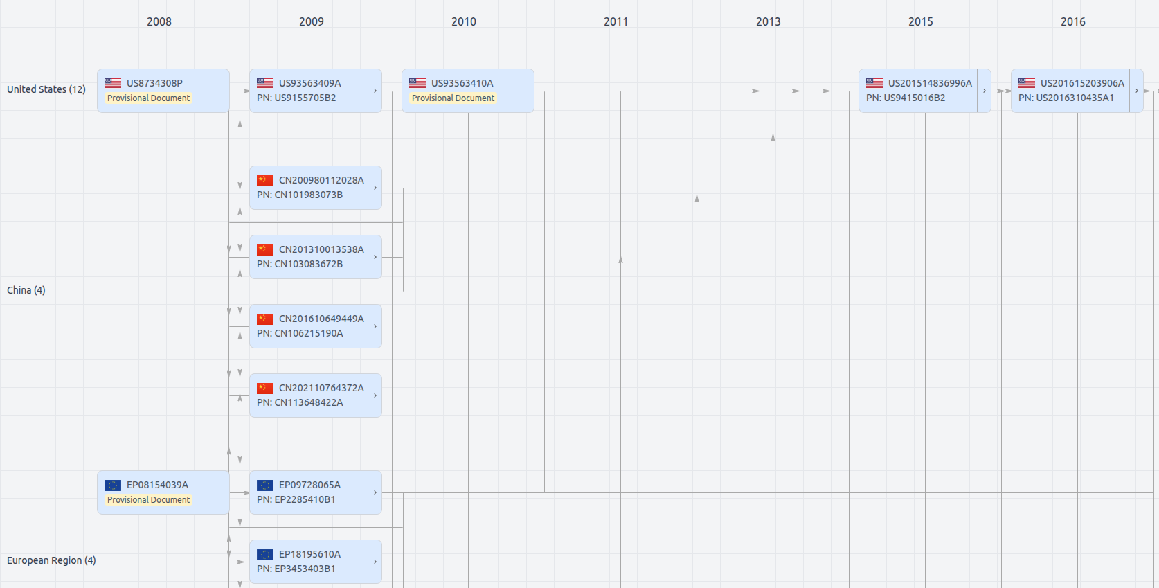
Patent Family

File Wrapper
The dossier documents provide a comprehensive record of the patent's prosecution history - including filings, correspondence, and decisions made by patent offices - and are crucial for understanding the patent's legal journey and any challenges it may have faced during examination.
Date
Description
Get instant alerts for new documents
US12094767
- Application Number
- US17580051
- Filing Date
- Jan 20, 2022
- Status
- Granted
- Expiry Date
- Dec 11, 2042
- External Links
- Slate, USPTO, Google Patents