Display Substrate And Display Device

Patent No. US12205506 (titled "Display Substrate And Display Device") was filed by Boe Technology Group Co Ltd on Mar 24, 2021.

What is this patent about?

’506 is related to the field of display technology, specifically addressing the design of a display substrate with an integrated gate driver on array (GOA) circuit. In modern displays, GOA circuits are used to sequentially activate gate lines, controlling pixel activation. A key challenge is maintaining stable output from the GOA circuit, especially during the 'keeping' phase where the output should remain constant despite noise and leakage currents. This is particularly important in displays using low-temperature polycrystalline oxide (LTPO) transistors, which require precise control to ensure consistent pixel charging.

The underlying idea behind ’506 is to improve the stability of the GOA circuit's output by incorporating a charge pump circuit within each shift register unit. This circuit, composed of capacitors and a transistor, boosts the potential of a critical node (the first node) during the keeping phase. By increasing the voltage level of this node, the transistor connected to it remains firmly on, effectively suppressing noise and maintaining a stable, low-voltage output signal. This ensures that the gate lines are reliably deactivated, preventing unwanted pixel activation and improving overall display quality.

The claims of ’506 focus on a display substrate featuring a shift register unit with a charge pump. The key elements include a first capacitor connected to a clock signal line and an input node, and a first transistor whose gate is connected to either its source or drain, forming a diode configuration. The claims emphasize the spatial arrangement of these components, requiring the first capacitor to be adjacent to the first transistor on the base substrate. Furthermore, the claims detail the connection of the transistor to the active layer through a via, ensuring that the channel region does not overlap with the via to avoid damage.

In practice, the charge pump circuit operates by using the clock signal to transfer charge to the first node, increasing its potential. The diode-connected transistor ensures that the charge remains trapped on the node, maintaining the boosted voltage during the keeping phase. The specific layout, with the capacitor adjacent to the transistor, is intended to minimize the area occupied by the circuit, allowing for a narrower bezel around the display. The use of a diode-connected transistor is a simple and effective way to achieve charge retention without requiring complex control circuitry.

A key differentiation from prior approaches lies in the specific configuration of the diode-connected transistor and the spatial arrangement of the capacitor and transistor. By ensuring that the via connecting the transistor to the active layer does not overlap with the channel, the patent aims to improve the reliability and performance of the transistor. The use of a three-capacitor structure connected in parallel further enhances the charge pumping capability, allowing for a more stable and noise-resistant output signal. This combination of circuit design and layout optimization contributes to a more robust and efficient GOA circuit for advanced display technologies.

How does this patent fit in bigger picture?

Technical landscape at the time

In the early 2020s when ’506 was filed, display technology commonly used gate drivers integrated on the array substrate (GOA) to drive gate lines. At a time when such GOA circuits were typically implemented using cascaded shift register units to provide on-off voltage signals to the gate lines.

Novelty and Inventive Step

The examiner approved the application because claims 5, 8, and 13, and claims depending from them, require a particular structural configuration and arrangement that was not taught or suggested by the prior art, either alone or in combination, without impermissible hindsight. The examiner considered the claimed arrangement to be a novel and non-obvious arrangement of elements.

Claims

This patent contains 20 claims, with independent claims 1, 18, and 19. The independent claims focus on a display substrate comprising a base substrate and a shift register unit with a charge pump circuit. The dependent claims generally elaborate on and add specific details to the elements and configurations described in the independent claims.

Key Claim Terms New

Definitions of key terms used in the patent claims.

Term (Source)Support for SpecificationInterpretation
Charge pump circuit
(Claim 1, Claim 18, Claim 19)
“the shift register unit comprises a charge pump circuit, the first clock signal line is configured to supply a first clock signal to the shift register unit, the first power line is configured to supply a first power voltage to the shift register unit, the charge pump circuit comprises a first capacitor, a first transistor, and a second capacitor, and the charge pump circuit is electrically connected with a first input node and a first node, respectively; For example, in some embodiments of the present disclosure, the charge pump circuit is configured to, under control of the first clock signal supplied by the first clock signal line during a first period, convert a potential of the first input node from a first voltage signal to a second voltage signal, and transmit the second voltage signal to the first node, and is configured to maintain a potential of the first node during a second period.”A circuit within the shift register unit that includes at least a first capacitor and a first transistor, and is electrically connected with a first input node and a first node. It is configured to convert a potential of the first input node from a first voltage signal to a second voltage signal, and transmit the second voltage signal to the first node, and is configured to maintain a potential of the first node during a second period.
First clock signal line
(Claim 1, Claim 18, Claim 19)
“At least one embodiment of the present disclosure provides a display substrate, comprising: a base substrate, and a shift register unit, a first clock signal line, and a first power line which are all provided in a peripheral region of the base substrate, wherein the shift register unit comprises a charge pump circuit, the first clock signal line is configured to supply a first clock signal to the shift register unit, the first power line is configured to supply a first power voltage to the shift register unit”A line provided in the peripheral region of the base substrate and configured to supply a first clock signal to the shift register unit.
First connection electrode
(Claim 1, Claim 18)
“the display substrate further comprises a first connection electrode and a second connection electrode; the gate electrode of the first transistor is connected with the first electrode of the first transistor through the first connection electrode to form a diode structure, a first end of the first connection electrode is connected with the first electrode of the first transistor, a second end of the first connection electrode is connected with gate electrode of the first transistor”An electrode that connects the gate electrode of the first transistor to the first electrode of the first transistor to form a diode structure.
First power line
(Claim 1, Claim 18, Claim 19)
“At least one embodiment of the present disclosure provides a display substrate, comprising: a base substrate, and a shift register unit, a first clock signal line, and a first power line which are all provided in a peripheral region of the base substrate, wherein the shift register unit comprises a charge pump circuit, the first clock signal line is configured to supply a first clock signal to the shift register unit, the first power line is configured to supply a first power voltage to the shift register unit”A line provided in the peripheral region of the base substrate and configured to supply a first power voltage to the shift register unit.
Structure of three capacitors connected in parallel
(Claim 19)
“at least one of the first capacitor and the second capacitor is a structure of three capacitors connected in parallel, and the structure of three capacitors connected in parallel comprises a first portion of the second electrode plate, a second portion of the second electrode plate, a first portion of the first electrode plate, and a second portion of the first electrode plate. For example, in some embodiments of the present disclosure, the first portion of the second electrode plate is connected with the second portion of the second electrode plate through a third via hole, the first portion of the first electrode plate is connected with the second portion of the first electrode plate through an connection portion, and the third via hole and the connection portion are respectively located on two opposite sides of the structure of three capacitors connected in parallel; and the first portion of the second electrode plate, the first portion of the first electrode plate, the second portion of the second electrode plate, and the second portion of the first electrode plate are arranged sequentially to form the structure of three capacitors connected in parallel, and the connection portion and the second portion of the second electrode plate are located in the same layer and insulated from each other.”A capacitor structure comprising a first portion of the second electrode plate, a second portion of the second electrode plate, a first portion of the first electrode plate, and a second portion of the first electrode plate, where the first portion of the second electrode plate is connected with the second portion of the second electrode plate through a third via hole, the first portion of the first electrode plate is connected with the second portion of the first electrode plate through a connection portion, and the third via hole and the connection portion are respectively located on two opposite sides of the structure.

Patent Family

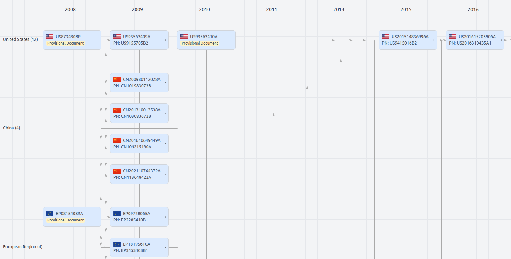
Patent Family

File Wrapper

The dossier documents provide a comprehensive record of the patent's prosecution history - including filings, correspondence, and decisions made by patent offices - and are crucial for understanding the patent's legal journey and any challenges it may have faced during examination.

  • Date

    Description

  • Get instant alerts for new documents

US12205506

BOE TECHNOLOGY GROUP CO LTD
Application Number
US17781988
Filing Date
Mar 24, 2021
Status
Granted
Expiry Date
Mar 24, 2041
External Links
Slate, USPTO, Google Patents